粉體行業在線展覽
粉體行業在線展覽


002


直接聯系
蘇州碳豐石墨烯科技有限公司


蘇州
面議
碳豐
002
131
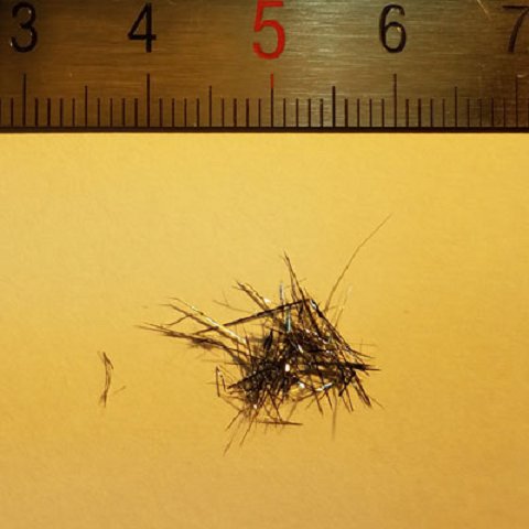
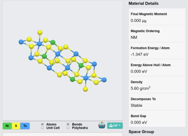
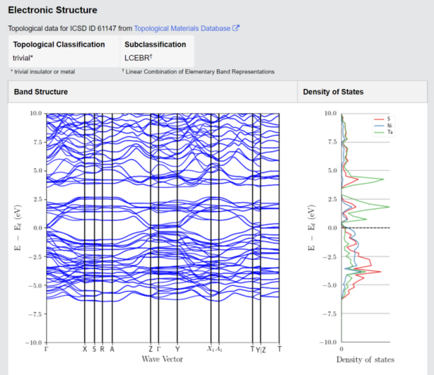
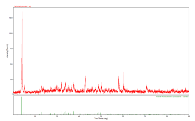
品名:TaNiS5 晶體
制造方法:
化學氣相沉積法, Chemical Vapor Deposition (CVD)
產品簡介:
| 晶體大小 | 3-10nm |
| 晶體種類 | Magnetic semiconductor |
| 純度 | >99.999% |
表征方法 | EDS,SEM,Raman |
晶體生長方式 | CVD化學氣相傳輸法 |
應用領域:
光電器件,微電子器件,生物傳感,化學傳感等領域。
參考文獻
1, Sunshine, Steven A., and James A. Ibers. "Structure and physical properties of the new layered ternary chalcogenides tantalum nickel sulfide (Ta2NiS5) and tantalum nickel selenide (Ta2NiSe5)." Inorganic Chemistry 24.22 (1985): 3611-3614.
2,Di Salvo, F. J., et al. "Physical and structural properties of the new layered compounds Ta2NiS5 and Ta2NiSe5." Journal of the Less Common Metals 116.1 (1986): 51-61.
3, Larkin, T. I., et al. "Infrared phonon spectra of quasi-one-dimensional Ta 2 NiSe 5 and Ta 2 NiS 5." Physical Review B 98.12 (2018): 125113.
4, Yan, Bingzheng, et al. "Ternary chalcogenide Ta 2 NiS 5 as a saturable absorber for a 1.9 μm passively Q-switched bulk laser." Optics letters44.2 (2019): 451-454.

有采購需求加微信咨詢